Hi @hfranco.tx,
Thank you for your response.
We still have some doubts regarding this topic.
Firstly, your answer regarding the typo on the wiki page is confusing us:
Although it’s saying it starts at 0x0000_0000, it’s not the same as the 0x0000_0000 from the Boot ROM.
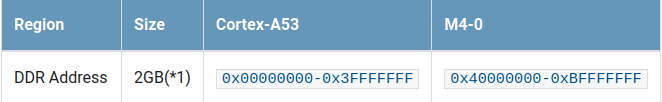
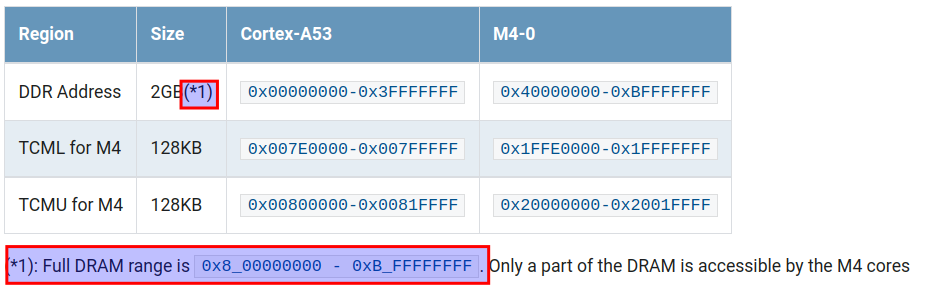
It says it starts from 0x8_0000_0000 and goes to 0xB_FFFF_FFFF (which is different from 0x0000_0000 to 0xFFFF_FFFF). Here I believe there is a typo, the NXP says it starts from 0x1_0000_0000 instead of 0x8_0000_0000. I’ll check that with the team and correct it.
If the address 0x8_0000_0000 is a typo and it should be 0x1_0000_0000, how to explain the end address of DDR range?
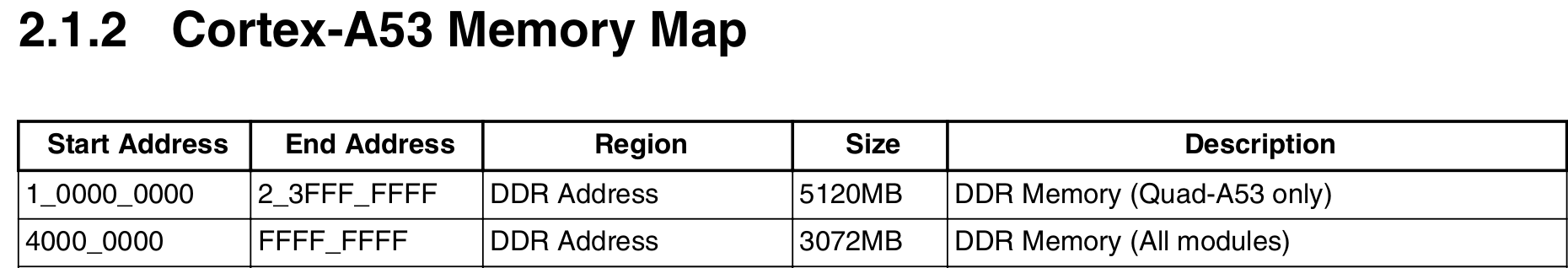
On the wiki page, it is 0xB_FFFF_FFFF, while in the reference manual, the end address of DDR range is 0x2_3FFF_FFFF. Moreover, DDR range from 0x1_0000_0000 to 0xB_FFFF_FFFF would mean that the total size of DDR is ~43 GB, which doesn’t make much sense.
Secondly, according to the reference manual, the DDR consists of two address spaces: 0x4000_0000 - 0xFFFF_FFFF and 0x1_0000_0000 - 0x2_3FFF_FFFF. This configuration implies that DDR can be accessed using 32-bit and 64-bit addressing.
How are DDR memory locations actually addressed by each core?
We presume that addressing is done by one of the two possibilities:
-
A53: 0x4000_0000 - 0xBFFF_FFFF (max. 0xFFFF_FFFF)
M4: 0x4000_0000 - 0xBFFF_FFFF
→ Physical memory locations are accessed by writing the same 32-bit memory address into the memory controller.
-
A53: 0x1_0000_0000 - 0x1_7FFF_FFFF (max. 0x2_3FFF_FFFF)
M4: 0x4000_0000 - 0x0xBFFF_FFFF
→ Physical memory locations are accessed by writing different memory addresses to the memory controller. More precisely, M4 and A53 write different 32-bit and 64-bit addresses, respectively, to the memory controller. In this case, if DDR physical address requested by the application from A53 and M4 are the same (e.g. DDR memory page at 0x1_0000), how are these addresses translated to respective 32-bit and 64-bit addresses (0x4001_0000 and 0x1_0001_0000)?
If the application is accessing the peripheral memory address 0x0000_0000 (boot ROM) and the DDR address “0x0000_0000” (we are not sure if the enquoted address is accessed at 0x4000_0000 or 0x1_0000_0000), how and when are these two addresses differentiated? Is the DDR address “0x0000_0000” somehow translated to 0x4000_0000 or 0x1_0000_0000?
Could you please clarify which of these approaches applies on iMX8M Mini platform? If none of the described approaches applies, could you please explain how is DDR memory addressing from different cores handled?
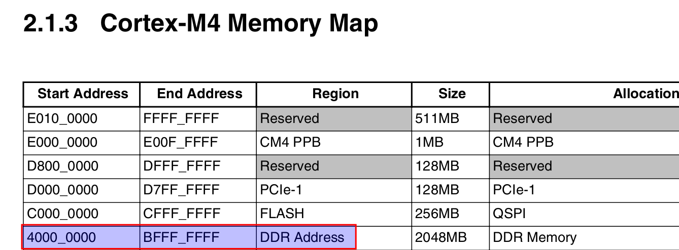
Thirdly, how to explain the configuration in the device tree, where it says that the RAM address space is from 0x4000_0000 to 0x8000_0000?
This configuration implies that the first approach described above is relevant.
In this case, how is the access to DDR through the memory controller handled - is the DDR addressed by 32-bit addresses or are they translated to 64-bit addresses at some point?