Enabling Second PCIe root complex in Apalis iMX8

Are there any instructions in this forum for how I can get a second PCIe root complex interface out of an Apalis iMX8 SOM?

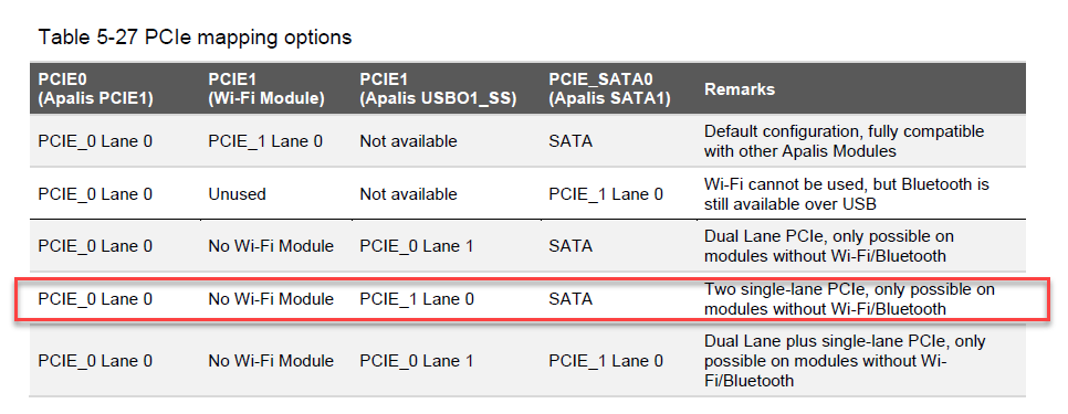
I’ve managed to find some resources on this forum about how one can enable a two lane PCIe root complex in an Apalis module.

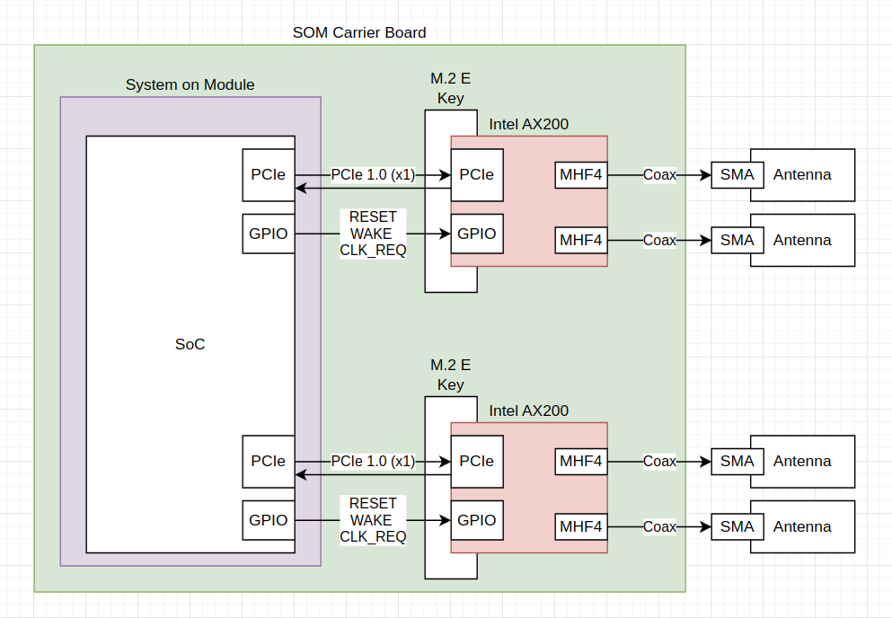
Currently working with the Apalis iMX8QM + Ixora breakout. I’m able to get both of my target PCIe endpoints working, one at a time, with the mini PCIe endpoint. What I need to do next is validate that I can speak to both of my endpoint devices at once with two separate PCIe root complexes.

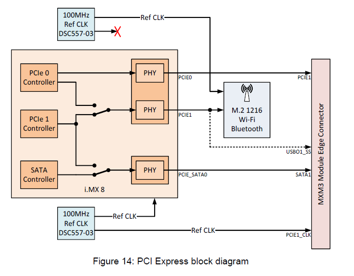
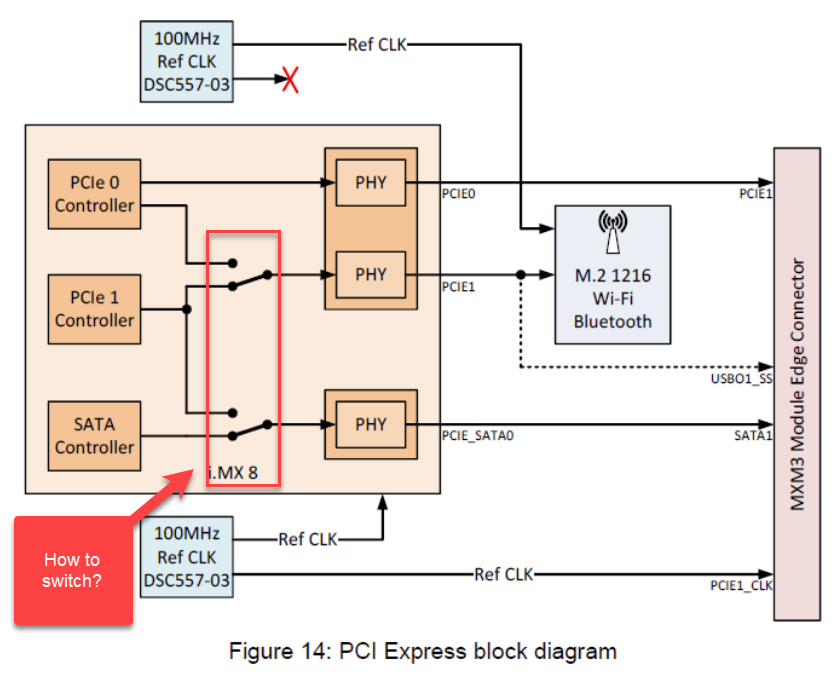
Based on prior experience bringing up second PCIe interfaces on other NXP chipsets, I think that would look something like this:

Hardware

  • Getting custom SOM with no wifi module populated
  • Add HCSL oscillator and/or fanout buffer to carrier board for reference clocks to both PCIe endpoints
  • Add GPIO for Reset, CLK_REQ, and WAKE_L to each individual PCIe endpoint

Software

  • Adding in device tree support for second PCIe interface
  • Modify IOMUX to enable PCIe pins
  • Disable SATA pins (could be same as IOMUX modifications)
  • (Potentially) enable PCIe in Uboot (have worked with some NXP chipsets that require this)

I was hoping I might get some more specific guidance from the Toradex folks on what needs doing - and, of course, make sure that my request is feasible.

Hey @nr-tst,

I don’t believe NXP supports dual/multi root complexes with PCIe. So I believe you won’t find any information on it. Usually the host contains/is the root complex, and PCIe devices connected are the endpoints.

Have you taken a look at our datasheet section 5.7 PCI Express for the IMX8 Apalis?

There are some limitations, but if you look at Table 5-27 PCIe Mapping, you’ll see the fourth option that allows for dual lane plus single plane PCIe.

There are IMX8 Apalis modules without the WiFI/Bluetooth module, but it isn’t for the highest RAM modules. ~ Apalis iMX8 QuadMax 4GB IT

And yes, there is a bit of hardware/software configuration required to get this setup.

You can reference our pinout designer tool to get an idea of the pin conflicts.
Pinout Designer, this and the Apalis datasheet are great resources.

I would also highly recommend looking at our Apalis Carrier Board Design Guide, specifically 2.2 PCI

-Eric

Hey Eric -

Thanks for the reply. Sorry it’s taken me a minute to get back to you. Things have been busy here, and I wanted to make sure my reply was thorough so that my questions were clear.

I think I may have used the term “root complex” too loosely in the original question. It’s probably helpful for me to start with the configuration I’m trying to achieve. Included a block diagram of that below:

Our goal is to use two Intel AX200s as discrete PCIe endpoints with the iMX8QM.

I think, based on this excerpt from the datasheet, that the line item boxed in red is the PCIe lane configuration on the SOM that I want to use:

If that’s the case, I have a followup question about how I’d refer to those signals in my carrier board in a way that matches Toradex’s convention. I’m confused as to how to reconcile Table 5-27 to Figure 14. To match the configuration I boxed in Table 5-27, my understanding is that we’d use a SOM that had no wifi module, which exposed the following peripherals to the SOM connector:

  • PCIe 0 Controller => PCIE0 (Chip Phy) => PCIE1 (Edge Cnxn)
  • PCIe 1 Controller => PCIE1 (Chip Phy) => USBO1_SS (Edge Cnxn)

If that’s the case - how do I map the USBO1_SS signals to PCIe signals? Here is my best guess given what I’ve seen:

MXM3 Pin Net PCIe Function
USBO1_SSTX_P PCIE_TX_P
USBO1_SSTX_N PCIE_TX_N
USBO1_SSRX_P PCIE_RX_P
USBO1_SSRX_N PCIE_TX_N

Given that, here’s my open questions:

  • Can you confirm the lane configuration I’ve shown here?
  • What’s your recommendation for routing PCIE_REF_CLK on the SOM in this case? I can see a few options:
    • Redistributing PCIE1_CLK (as specified in Figure 14) through a fanout buffer
    • Generating the REF_CLK on the board with an HCSL oscillator, and fanning it out thru a buffer to the M.2 cards there
    • Generating REF_CLK thru dedicated HCSL osc to each M.2 card (I don’t want to do this unless as a last resort, for cost and technical reasons)
  • What sort of software modifications would my team need to make in order to enable the functions I described in this question?
  • Would it be easier for you to simply review a schematic we sent you? I can implement the subset I’m concerned about and send it off to you in the next few working days.

Hey @nr-tst,

As I look into this, I just wanted to tell you about our pinout designer tool that can really assist with pin muxing.

Yes, if you want each endpoint to have 1 lane this is the correct one.

Take a look at 2.2.2 Reference SChmatics for PCIe on the apalis arm carrier board design, this has some information that will help.

Device tree modifications are the start, with a focus on pin multiplexing to get the correct pins functions.

Sure, depending on how complex it is, we sometimes have the ability to do quick reviews to more complex paid ones. I would send this privately though rather than through our public forums.

-Eric

Hey Eric -

Bringing this up again, as we are trying to figure out how to connect the PCIe1 controller to the PHY block that drives PCIE_SATA0:

So far we don’t have any bright ideas of how to do this besides disabling the SATA controller.

Looking through the toradex source tree, this appears like it might be the configuration we want, we’re just not certain how to apply it to our hardware:

// SPDX-License-Identifier: GPL-2.0+
/*
 * Copyright 2020 NXP
 */

/dts-v1/;

#include <dt-bindings/usb/pd.h>
#include "imx8qm-mek.dts"

/*
 * Add the PCIeA x2 lanes and PCIeB x1 lane usecase
 * hsio-cfg = <PCIEAX2PCIEBX1>
 * NOTE: In this case, the HSIO nodes contained
 * hsio-cfg = <PCIEAX1PCIEBX1SATA> would be re-configured.
 */
&pciea{
	ext_osc = <1>;
	pinctrl-names = "default";
	pinctrl-0 = <&pinctrl_pciea>;
	disable-gpio = <&lsio_gpio4 9 GPIO_ACTIVE_LOW>;
	reset-gpio = <&lsio_gpio4 29 GPIO_ACTIVE_LOW>;
	epdev_on-supply = <&epdev_on>;
	num-lanes = <2>;
	clocks = <&pciea_lpcg 0>,
		 <&pciea_lpcg 1>,
		 <&pciea_lpcg 2>,
		 <&phyx2_lpcg 0>,
		 <&phyx2_crr0_lpcg 0>,
		 <&pciea_crr2_lpcg 0>,
		 <&misc_crr5_lpcg 0>;
	clock-names = "pcie", "pcie_bus", "pcie_inbound_axi",
		      "pcie_phy", "phy_per","pcie_per", "misc_per";
	hsio-cfg = <PCIEAX2PCIEBX1>;
	status = "okay";
};

&pcieb{
	ext_osc = <1>;
	clocks = <&pcieb_lpcg 0>,
		 <&pcieb_lpcg 1>,
		 <&pcieb_lpcg 2>,
		 <&phyx1_lpcg 0>,
		 <&phyx2_lpcg 0>,
		 <&phyx1_crr1_lpcg 0>,
		 <&pcieb_crr3_lpcg 0>,
		 <&pciea_crr2_lpcg 0>,
		 <&misc_crr5_lpcg 0>;
	clock-names = "pcie", "pcie_bus", "pcie_inbound_axi",
		      "pcie_phy", "pcie_phy_pclk", "phy_per",
		      "pcie_per", "pciex2_per", "misc_per";
	power-domains = <&pd IMX_SC_R_PCIE_B>,
			<&pd IMX_SC_R_PCIE_A>,
			<&pd IMX_SC_R_SERDES_0>,
			<&pd IMX_SC_R_SERDES_1>,
			<&pd IMX_SC_R_HSIO_GPIO>;
	power-domain-names = "pcie", "pcie_per", "pcie_phy",
			     "pcie_serdes", "hsio_gpio";
	hsio-cfg = <PCIEAX2PCIEBX1>;
	status = "okay";
};

&sata {
	status = "disabled";
}

(Referenced from: imx8qm-pcieax2pciebx1.dts « freescale « dts « boot « arm64 « arch - linux-toradex.git - Linux kernel for Apalis, Colibri and Verdin modules)

Question 1: How could we flip that internal switch and connect PCIe1 controller to the PCIE_SATA0 phy?
Question 2: Can you advise how to apply the device tree setting above to our software?