Verdin iMX8M Mini: JTAG Boundary Scan

Hello

We are currently using the Verdin iMX8MM Q 2GB IT (V1.1C).

Is it possible to set the module to JTAG boundary scan mode?
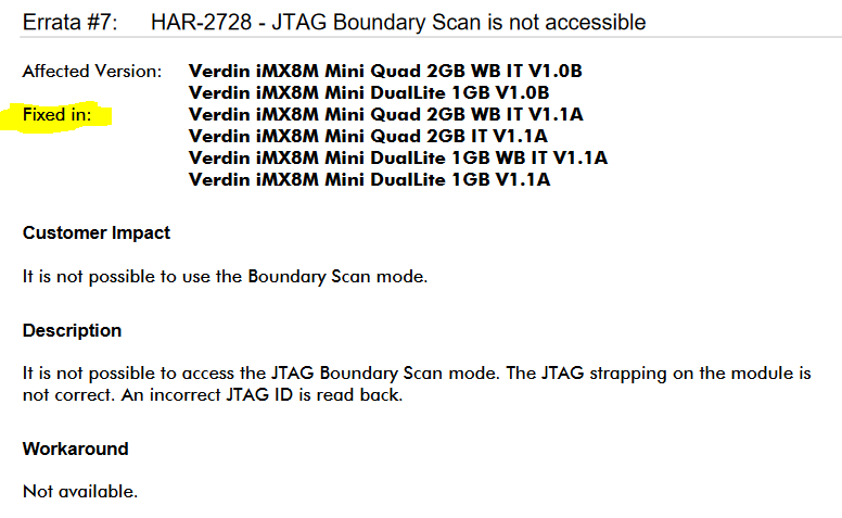
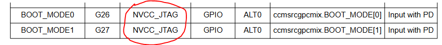
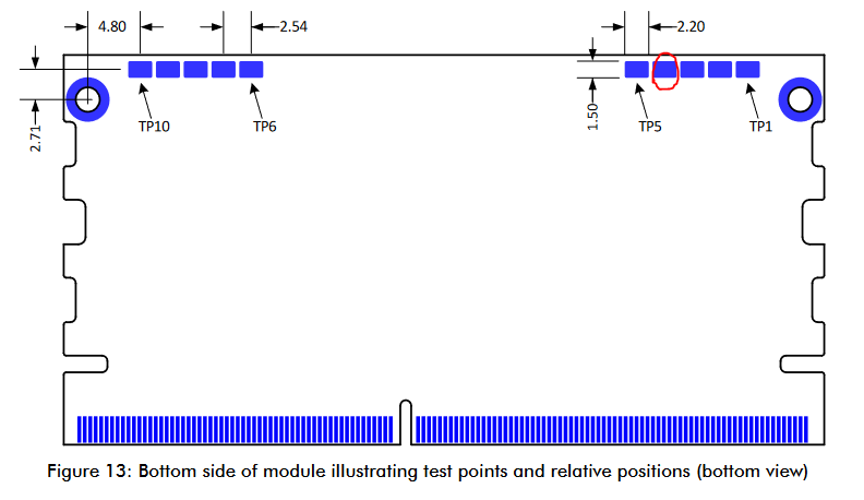
The Errata (https://docs.toradex.com/107330-verdin-imx8m-mini-errata.pdf) states (Errata #7) that this mode should be accessible on the new variant. However, as I have seen in the datasheet, the iMX8 pin “BOOT_MODE1” on the Verdin board is pull-downed. Might it be necessary to do something with the 10 test points on the back side of the module?

Hi @Aeni !

Thanks for reaching out to Toradex Community :slight_smile:

I think you are referring to this page of Verdin iMX8MM’s datasheet (available at Verdin iMX8M Mini | Toradex Developer Center), right?

I just could not find where the image you shared came from. Could you specify?

Best regards,

Hi @henrique.tx

Yes I got the configuration of BOOT_MODE1 from the Verdin datasheet.

The image I got from the " i.MX 8M Mini Hardware Developer’s Guide" (Document identifier: IMX8MMHD: Sign in to NXP.com | NXP Semiconductors): Table 17

Best regards,

Hi @Aeni !

Seems like there is not much to do.

The modules are strapped via hardware to configure the boot and BOOT_MODE1 is, as you saw, pulled-down.

Could you share what is your use case and why you would like to use boundary-scan on the module?

Best regards,

Hi @henrique.tx
Our manufacturer usually checks the assembled PCB with boundary scan.

But why does the errata state that the JTAG boundary scan should now be available? That is confusing …

Best regards,

Hi @Aeni !

After asking internally, there is a step-by-step for it:


Verdin iMX8MM - Boundary Scan

These are the steps to verify if boundary scan is working:

  1. Connect the JTAG Interface to Carrier Board.
  2. Connect TP4 to 3.3V either connecting a direct cable or using the POGO Pins on the Development Carrier Board.
  3. Connect the CTRL_RECOVERY_MICO (SODIMM246) to GND.
  4. Boot the SoM. The SoC will be in Test mode which is different than the recovery mode.
  5. Run the Windows Application Top JTAG Probe.
  6. Load the Verdin iMX8MM Project.
  7. Click on Instruction and choose EXTEST and “Use safe values from the device BSDL file”
  8. After clicking OK, press Run.

Now can choose a PIN to toggle. Just be aware not to short circuit a PIN on the SOM and/or turn off a PIN which is needed for the Power up of the Soc. For example, we used SODIMM53:i2c2_sda (SoC:D10) and SODIMM55:i2c_scl (SoC: D9), which is safe to use, since these pins have a pull up resistor.

You can use the pin from the Top JTAG Probe tool to be an input or output.

  • When the PIN is used as an output, you can drive a LED with this.
  • For Input you can either pull the pin up to 3.3V or GND and readout the value inside the Application.

As I do not have a JTAG, I wasn’t able to test it myself.

Does it help you?

Best regards,

PS: the Verdin iMX8MM Project will be available for 1 year from today.

Hi @henrique.tx

Thank you for your answer!

Can the TP4 really be connected to +3V3? I ask because this pin is connected to the same power domain as the JTAG (NVCC_JTAG) and this domain is +1V8 as far as I know. Or do you have some kind of buffer between?


(Source: Datasheet iMX8M Mini, Table 67)

As a precaution, I connected the pin to +1V8 and it worked. I was then able to toggle the corresponding pins and read out an EEPROM via I2C. I used a different tool than you (GitHub - viveris/jtag-boundary-scanner: JTAG boundary scan debug & test tool.). But in the end it does the same thing.

Info for the others: The TP4 is located here:


(Source: Verdin Family Specification)

Best regards,

After asking internally, I was told that although people here tested with 3.3V (and it worked), 1.8V should work as well.

So it worked for you?

Best regards,

Hi @henrique.tx ,

Yes it worked.
I will mark your answer as the solution.

Thank you very much!

Best regards,

1 Like

Hi @Aeni !

Thanks for the feedback!

Have a nice day! :smiley:

Best regards,

Hi @henrique.tx ,

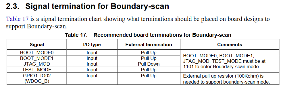
I have a small follow-up question regarding this topic: Are the other 3 pins (JTAG_MOD, TEST_MODE, GPIO1_IO02) actually wired according to NXP’s boundary-scan specification on the Verdin iMX8M Mini (see picture in the initial question)? Like this:

  • JTAG_MOD: Pull-Down
  • TEST_MODE: Pull-Up
  • GPIO1_IO02: Pull-Up

Best regards,

Dear @Aeni ,

  • JTAG_MOD has a 10k pull down resistor and can be controlled through the connection to to TP3.
  • TEST_MODE is connected to BOOT_MODE1 with a 10k pull down resistor and can be controlled through the connection to TP4.
  • GPIO1_IO02 is connected to PMIC_WDI and has a 100k pull up resistor to 1.8V.

This has been done to not statically enter the boundary scan mode. From Version 1.1 onward an errata has been issued, which enables you to access the mode via the TPs.
I hope this answers your questions.

Best regards
Collin

1 Like