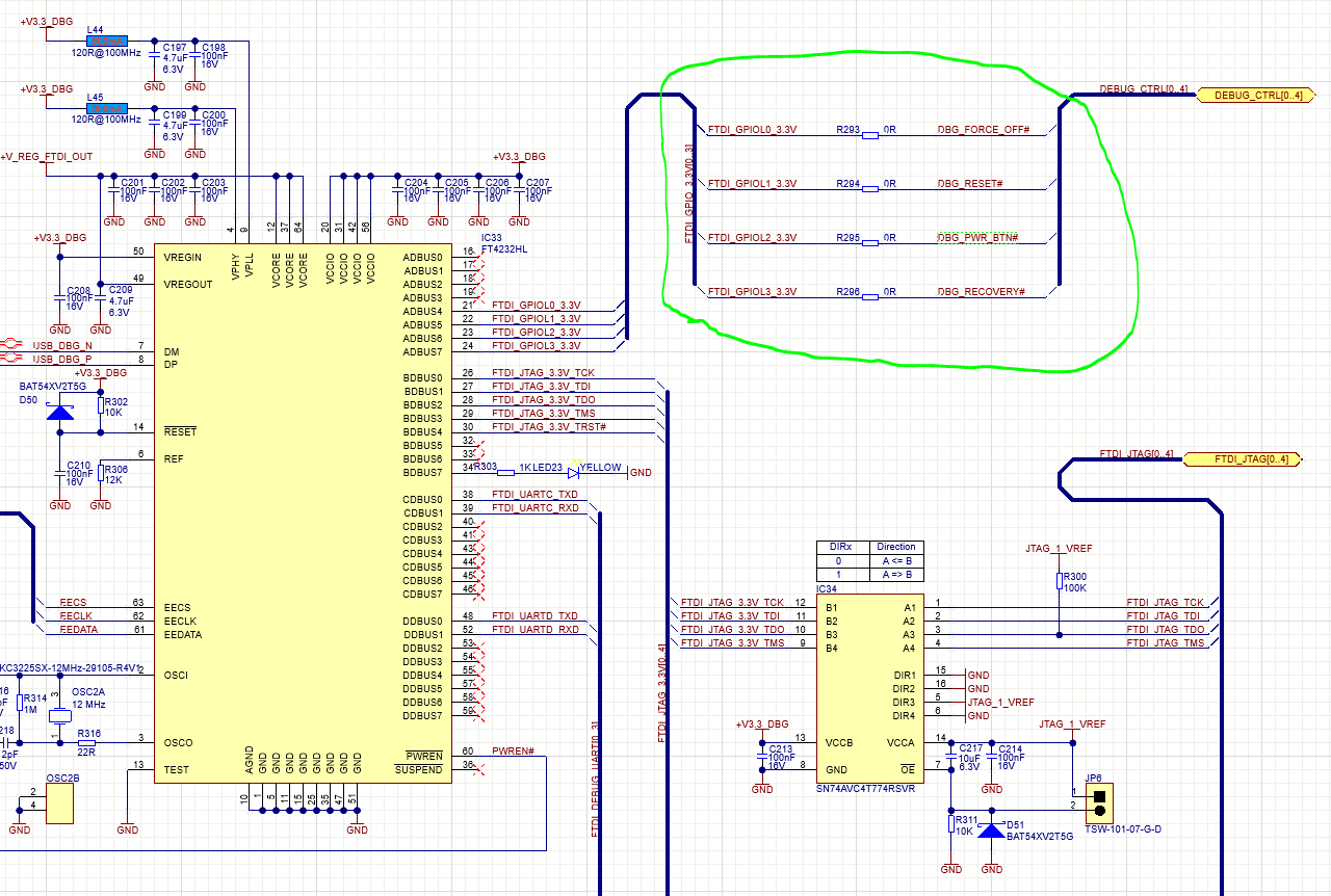
I’m developing a board starting off with the Dahlia Carrier board Rev. 1.1. I’m wondering if the “DBG_FORCE_OFF#/DBG_RESET#/DBG_PWR_BTN#/DBG_RECOVERY#” signals are necessary. According to the schematics, these signals fulfill the same function as the SW1, SW3 and SW5 switches, except for the DBG_FORCE_OFF# signal that is connected to the KILL input of the pushbutton on/off controller.
I could not find documentation about these signals anywhere so I do not know if they are necessary for something or I can remove them from the schematic. How are these signals controlled from the PC?
On the other hand, I understand that to debug this module, only the JTAG, the UART_3 and the UART_4 are necessary.