G’day,
I’m just about finished with the schematics for my custom Apalis carrier board, and am hoping to have some input regarding my proposed board layout from an embedded engineer more experienced than myself. To begin with, here’s the proposed layout:
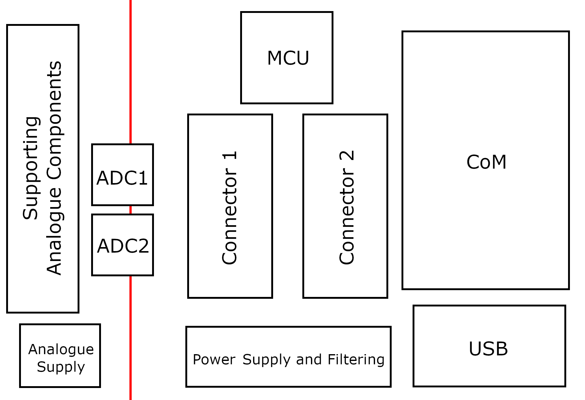
A couple of notes on the layout:
- Connector 1 and Connector 2 provide both power and signals to the board, and their position is a hard requirement (i.e. they cannot be moved).
- All other components can be moved as recommended.
- Everything to the left of the red line is analogue, everything to the right is digital.
- The 2 ADCs straddle the analogue/digital line, with their analogue and digital pins on the respective side of the line.
- This is a 4 layer board (Component/Signal, GND, Power, Signal). The GND plane is a continuous solid, with the analogue/digital line representing a theoretical split in the plane only (i.e. there are no cuts, splits, etc. in the GND plane to separate the analogue and digital GNDs).
- Components are only to be placed on the top surface.
- The analogue components are powered by a separate analogue supply (bottom left corner).
- The ‘Power Supply and Filtering’ uses various protection diodes, CLC filters and buck/buck-boost converters to provide the board with the required 12V, 5V and 3V3 sequenced supplies.
- The MCU does the majority of the computation and speaks with the Apalis CoM via a direct ethernet connection.
- Not shown are WiFi/Bluetooth and CAN hardware.
My major considerations in the layout are as follows:
- Separation of analogue and digital circuits to minimise crosstalk and EMI.
- Careful planning of current return paths, accounting for both low frequency/DC return paths (i.e. least resistance point to point) and high frequency return paths (i.e. least impedance following the signal trace).
Does the above make sense and is it a reasonable layout? As mentioned above, with the exception of Connector 1 and 2, I am free to move components/modules around as needed.
Thanks!